Introduction
Switching power supplies are essential components in multiple modern electronic devices, providing efficient power conversion and regulation. Though these components have a multitude of uses in varied industrial machinery and consumer electronics, their performance can be significantly affected by parasitic components––leading to significant losses, noise, and instability. This article discusses key strategies and design considerations for minimizing these parasitic components to enhance the performance and reliability of switching power supplies.
Introduction to Switching Power Supplies: Types and Applications
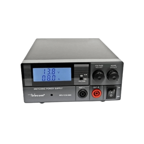
Switching power supplies, also called Switch-Mode Power Supplies (SMPS), are a type of power supply unit (PSU) used in a myriad of electronic devices to convert electrical power efficiently. Unlike linear power supplies, which regulate output voltage through dissipative techniques, switching power supplies use a high-frequency switching circuit to convert the input power to the desired output voltage and current levels with higher efficiency.
Some of the popular switching power supplies include AC-DC converters, DC-DC converters, LED drivers, laptop chargers, power inverters, forward converters, flyback converters, and push-pull converters. These power supplies are found in a variety of applications, including computer power supplies, battery chargers, telecommunications equipment, and medical devices. Their efficiency and compact size make them suitable for portable and energy-sensitive applications.
Understanding Parasitic Components: Causes and Effects
Parasitic components, also called parasitics, are unintended electrical elements that exist within a circuit or device due to the inherent properties of components and their physical layout. These components render unintended electrical properties and behaviour that are not part of the intended design. Parasitic components in power supply can arise from various sources, including PCB traces, semiconductor devices, and passive components. These parasitics can lead to multiple issues in switching power supplies, including:
- Reduced Efficiency: Parasitic components can introduce additional resistance, capacitance, or inductance, leading to increased power losses and reduced overall efficiency in the power supply.
- Voltage Spikes and Noise: Parasitic capacitance and inductance can cause voltage spikes and electromagnetic interference (EMI), potentially affecting the operation of sensitive electronic components in the system.
- Stability Problems: Parasitics can lead to instability in the control loop of the switching power supply, causing oscillations, voltage overshoots, or undershoots and compromising the supply’s ability to maintain steady output voltages.
To create efficient and reliable switching power supplies, designers must consider these parasitic components and implement strategies to minimize their effects.
Best Strategies for Minimizing Parasitic Components
Minimizing parasitic components is crucial in electronics and electrical engineering to improve the performance and reliability of circuits and systems. Parasitic components, such as parasitic capacitance, inductance, and resistance, can significantly affect the behaviour of a circuit, leading to issues like unwanted oscillations, signal degradation, and power loss. Here are strategies for minimizing these parasitic components:
Component Selection
Selecting high-quality components is essential for minimizing parasitic components in switching power supplies. Opt for components with low equivalent series resistance (ESR), low equivalent series inductance (ESL), and low parasitic capacitance to ensure the components themselves introduce minimal parasitic effects.
PCB Layout
Proper printed circuit board (PCB) layout is crucial in minimizing parasitic components. Some key layout considerations include:
- Component Placement: Place critical components, such as capacitors and inductors, as close as possible to the switching elements and load to minimize trace lengths and reduce parasitic effects.
- Ground Plane: Implement a dedicated ground plane on the PCB to provide a low-impedance return path for high-frequency currents and reduce ground loop effects.
- Keep Traces Short: Keep traces for high-frequency signals as short as possible to reduce parasitic inductance.
Snubber Circuits
Snubber circuits are designed to absorb energy and reduce voltage spikes and ringing caused by parasitic components. These circuits typically consist of resistors and capacitors strategically placed across specific components to dampen transient behaviour.
Magnetic Components
Select magnetic components (inductors and transformers) carefully, considering factors like core material, winding techniques, and the number of turns. High-quality magnetic components with low parasitic effects can dramatically improve the overall performance of the power supply.
EMI Filters
EMI filters can help reduce radiated and conducted noise caused by parasitic components. These filters include passive components like ferrite beads, common-mode chokes, and capacitors designed to filter out high-frequency noise.
Simulation and Testing
Before finalizing a switching power supply design, use simulation tools to model parasitic effects and evaluate the circuit’s behaviour. Conduct rigorous testing to ensure the power supply meets performance specifications and complies with regulatory standards.
Optimizing Control Loop Design
Optimizing control loop design for mitigating parasitic components requires a combination of careful component selection and control techniques, such as:
- Adaptive Control Techniques: Implement control techniques that can adapt to changes in load and input conditions, compensating for the effects of parasitic components.
- Stability Analysis: Perform stability analysis to ensure the control loop can handle the dynamics introduced by parasitic components without becoming unstable.
Final Words
Minimizing parasitic components is essential in designing efficient and reliable switching power supplies. A well-designed switching power supply not only enhances the performance of electronic devices but also contributes to overall system reliability and longevity. By carefully selecting components, optimizing PCB layouts, using snubber circuits and compensation techniques, choosing magnetic components wisely, incorporating EMI filters, and conducting thorough simulations and testing, engineers can mitigate the adverse effects of parasitics and create power supplies that deliver stable, efficient, and noise-free performance.


